|
From 1999 to 2001 I worked on the DARPA-funded 3DMEMS
program at the University of
Maryland. My advisor was Prof. Don DeVoe.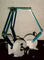
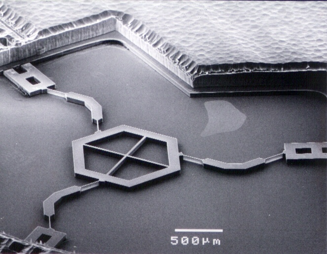
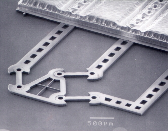
Pictured at left is a 3-DOF parallel manipulator originally
designed by Prof.
Lung-Wen Tsai and prototyped by Rick Stamper
at the University
of Maryland. The 3DMEMS effort began as a collaboration between
Prof. DeVoe's MEMS group and Prof. Tsai's mechanisms group.
As envisioned by DeVoe and Tsai, the primary goal
of the 3DMEMS program is to develop, demonstrate, and apply a batch
fabrication process to construct 3-D microsystems. The process takes
advantage of recent developments in silicon-based fabrication technology
such as fusion bonding and deep reactive ion etching (DRIE). This
research is expected to enable batch fabrication of mechanically robust
micromechanisms that are capable of true 3-D motion
The essential ideas of the 3DMEMS process are:
-
Robust, true 3-D capability: A true 3-D fabrication
process must be capable of producing devices with characteristics
such as overhangs, out-of-plane joints, and enclosed cavities.
The traditional criticism of MEMS is that devices are simply
extrusions of 2-D patterns.
This is certainly the case when bulk micromachining processes
such as DRIE are used without any modifications. While multi-layer
processes such as MUMPs®*
and SUMMiT
can be used to produce true 3-D devices, the thin structural layers
associated with surface micromachining are extremely compliant. The
3DMEMS process combines the mechanical strength of
high-aspect-ratio devices with the true 3-D capability of
multi-level processes.
*Note: this overview
was written in 2001. A MUMPs process (SOIMUMPs) now exists wherein
users can create high-aspect-ratio structures.
-
Silicon-on-insulator
(SOI) wafers: Single crystal silicon (SCS) was chosen as
the 3DMEMS structural material because of its favorable
mechanical and electrical properties. 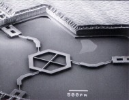 For example, SCS has no
grain boundaries, making it a perfectly elastic material.
Additionally, silicon possesses a stable, insulating
oxide. SOI wafers feature a thin silicon layer separated from a
thick silicon substrate by an oxide layer. Because the 3DMEMS process uses two SOI wafers, only
one aligned bonding step is required to produce several
structural layers. For example, SCS has no
grain boundaries, making it a perfectly elastic material.
Additionally, silicon possesses a stable, insulating
oxide. SOI wafers feature a thin silicon layer separated from a
thick silicon substrate by an oxide layer. Because the 3DMEMS process uses two SOI wafers, only
one aligned bonding step is required to produce several
structural layers.
-
Batch fabrication:
Once masks are produced for photolithography, subsequent process
steps fabricate all the devices on the wafer simultaneously.
Although many 3-D microfabrication processes have been explored
by other groups, most require individual or sequential device
fabrication, which increases manufacturing time and expense. The
use of batch fabrication permits the simultaneous fabrication of
hundreds or thousands of devices.
-
Parallel manipulation: In general, manipulators can be
fabricated in either serial or parallel configurations. A
parallel manipulator allows multiple degrees of freedom to be
attained while all of the actuators remain on the base. In
contrast, a multiple-DOF serial manipulator requires some form
of actuation at the intermediate joints. Since it is not practical
in our case to
mount microactuators on moving links, all control
inputs to the micromanipulator must originate from the fixed base.
-
Linear actuation: Tsai's 3-DOF parallel
manipulator employs rotational electromagnetic actuators to position the platform. At the
micro-scale, however, it is easier to design and fabricate a linear
actuator. Our design uses linear 1-DOF slider inputs. We chose
electrothermal motors as an actuation method because they can produce
relatively high forces and are relatively simple to fabricate. In
fact, our electrothermal linear motor design
is very compatible with the 3DMEMS fabrication process, requiring only
the addition of a metallization step to create bond pads.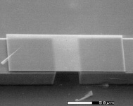
-
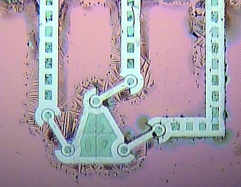
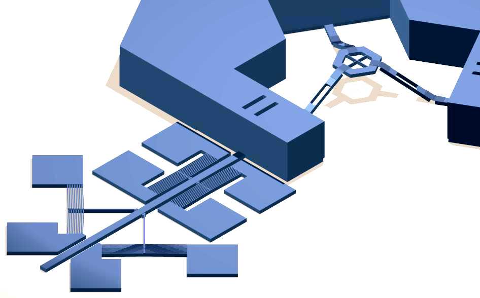
Compliant joints: The macro-scale version
uses hinges to achieve in-plane and out-of-plane
motion. Our design replaces these hinges with compliant, or
flexural, beams. A close-up view of an out-of-plane joint is shown
at right. Compliant beams can be used to mimic the
behavior of hinges without the associated "slop" resulting
from clearances between hinge components. Part of the 3DMEMS
research program involves modeling the
behavior of compliant joints.
A large portion of my graduate work involved
developing
and refining the 3DMEMS process. Around April 2001, when I
graduated, we wrapped up the first fabrication run, completing the
first out-of-plane joints. This joint was constructed by bonding together
the patterned active layers of two SOI wafers. The actual joint, which
is only 2 microns thick, is part of the active layer of the top SOI
wafer. The substrate of that wafer is used to form caps that hold
the sliders in place.
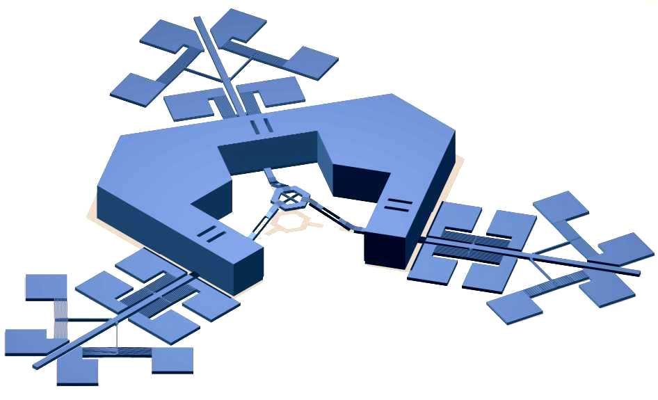
Shown below are conceptual views of a
three-degree-of-freedom (3-DOF) spatial platform micromanipulator
(images rendered in AutoCAD 2000 from the original design files). This
device was designed by Zhongzhou Tang and me. A spatial manipulator is
just one example of a device that can be fabricated using the 3DMEMS
process. Envisioned applications for similar devices include sample
positioners for scanning electron microscopes, tools for
minimally-invasive surgery, and dexterous linkages for
microrobots.
All 3-D microfabrication was
conducted with the help of my colleagues Dave Schreiber and Brett
Piekarski of the Maryland MEMS Lab.
Some fabrication was performed at the Army
Research Laboratory. The
assistance of Tom Loughran and Nolan Ballew is gratefully
acknowledged.
|