Back to table of contents | Next section
2.3 3DMEMS Process Flow
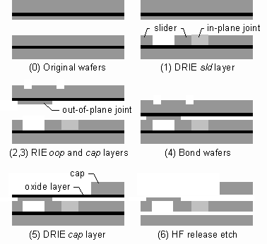
The 3DMEMS process flow is discussed in this section. The original fabrication process steps are listed in Table 1.
Table 1. 3DMEMS process flow (P = pattern, AP = aligned pattern).
|
Step |
Layer |
Process |
Comments |
|
1 |
sld |
P / DRIE 50 mm |
Define slider and guides |
|
2 |
oop |
P / RIE 2 mm |
Define out-of-plane joints |
|
3 |
cap |
AP / RIE 1 mm |
Etch alignment marks |
|
4 |
sld / oop |
Clean, align, bond |
|
|
5 |
cap |
AP / DRIE 525 mm |
Define cap |
|
6 |
all |
HF etch |
75 mm timed etch |
The fabrication process is illustrated in Figure 9. These illustrations represent a sectional view down the length of one of the input sliders. In step 1, the slider and guides are defined by a 50 mm etch of the first SOI wafer down to the buried oxide layer. In step 2, the out-of-plane joints are defined by a 2 mm etch of the second SOI wafer down to the oxide. In step 3, the cap layer is aligned to the oop layer. After being patterned on the back of the second wafer, the cap layer is etched 1 mm to provide alignment marks for steps 4 and 5.
Figure 9. Illustration of 3DMEMS process flow.
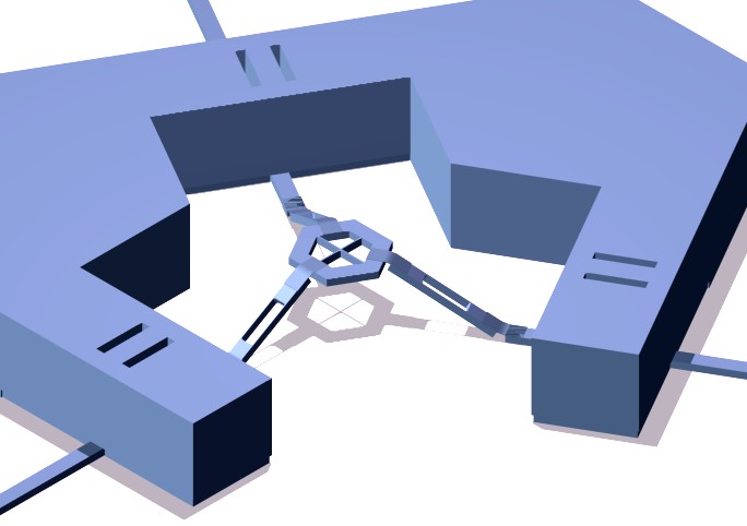
In step 4, both wafers are cleaned and activated by means of the RCA treatment. The wafers are then aligned and contacted in an optical aligner and then annealed in an oven for one hour at 1000 °C. In step 5, the cap layer is repatterned on the back of the second wafer over the existing 1 mm cap layer patterns. DRIE is then used to etch entirely through the substrate, creating the caps. Finally, a timed HF etch is used to remove the exposed oxide and release the sliders and platform. The anchors and cap are large enough to prevent them from being undercut entirely. The released platform is then free to move out of the wafer plane. A conceptual view of a device with a raised platform is shown in Figure 10.
Figure 10. Complete conceptual view of 3DMEMS platform micromanipulator based on actual process flow.