Back to table of contents | Next section
2.4 Design Rules and Process Details
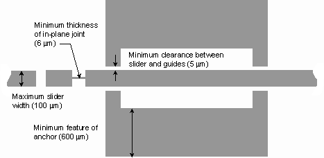
To ensure successful fabrication, it is necessary to develop design rules to ensure that features are properly etched and that the correct structures are released during the HF etch step. Most design rules emerge from the process limitations of lithography, wafer alignment and bonding, and DRIE. Some of the design rules that apply to the sld layer are shown in Figure 11.
Figure 11. Selected design rules of the sld layer.
The maximum slider width is 100 mm to ensure that it is released during the HF etch step. Because the slider only needs to be etched 50 mm from each side, the 75 mm timed etch represents a factor of safety of 50%. Conversely, the anchors have a minimum size of 600 x 600 mm to prevent release. The minimum gap and beam width of 5 mm and 6 mm are set by lithography and DRIE limitations. An inset is etched into the anchor to allow HF access to the slider during release. A complete explanation and listing of the design rules associated with all three layers can be found in Appendix A.
Lithography was performed at the Institute for Plasma Research (IPR) at the University of Maryland. A thick-film photoresist, AZ9245, was used as a mask for subsequent RIE and DRIE steps. A diluted mixture of 400K developer was used to develop the exposed photoresist.
RIE was performed at IPR on a Trion Minilock etcher. DRIE was performed courtesy of the Army Research Laboratory on a Plasma-Therm etcher at the Johns Hopkins Applied Physics Laboratory (APL). Aligned lithography and bonding were performed at APL on a Karl Suss MA/BA6 optical aligner/bonder.
Appendix B contains a detailed description of the basic processes, such as lithography, wafer cleaning, reactive ion etching, and HF etching, that are incorporated in the 3DMEMS process. The wafers and photomasks used in the process are also described.