A.1 Explanation and Origin of Design Rules
Design rules have been developed to ensure correct 3DMEMS device fabrication. Design rules are derived from information on the limitations of the lithography, etching, aligning, and release processes. Design rules for the sld, oop, and cap layers are explained in this appendix.
Design rules often set minimum and maximum feature dimensions. For example, gaps less than 5 mm wide may not be resolved during lithography; beams less than 6 mm wide may not survive the DRIE step due to the bowing and footing effects and photoresist erosion [12]. Additionally, devices must be sized with a factor of safety to be released or remain anchored during HF etching. The 75 mm timed HF etch was designed to release structures smaller than 100 mm, as etching occurs from all sides. Conversely, anchors should be 600 mm or greater on each side to avoid release.
Some rules exist to prevent mechanical failure. To reduce stress concentrations, 6 mm chamfers are required where an in-plane joint meets a slider. Because the compliant joints are expected to perform at angles exceeding 45 degrees, stress due to large bending moments must be considered. Assuming constant bending moment and ignoring other loads, the maximum stress in a compliant beam is derived as
(46)

where q is the angle of deflection. Using a yield stress sy of silicon of 7.0 GPa, the minimum length-to-width ratio for a deflection of 90 degrees is calculated as approximately 19 [4]. To provide a factor of safety, the design rules dictate length-to-width ratios exceeding 30.
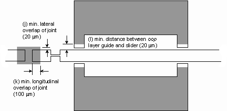
Rules can also concern the positioning of certain features. Errors up to 10 mm must be anticipated when performing optical alignment for lithography and bonding. These errors, which compound when successive layers are aligned, can be accommodated by making the out-of-plane joints larger than necessary to ensure complete coverage of the slider during bonding.
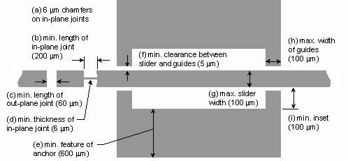
Design rules associated with the sld layer are illustrated in Figure 38. Rule (a) requires chamfers on in-plane joints to reduce stress concentrations. Rules (b) and (c) dictate minimum joint lengths to reduce bending stresses. Rules (d) and (f) concern minimum feature sizes, and Rules (e) and (g) concern released and unreleased feature sizes. Rule (h) sets the maximum width of the guides to allow HF access to the adjacent slider area. Finally, Rule (i) dictates a minimum inset size to accommodate the HF etch holes created in the oop and cap layers.