Back to table of contents | Next section
1.2 General Microfabrication Background
This section is intended to provide an overview of common micromachining techniques involving SCS and polycrystalline silicon (polysilicon) as a background for describing the 3DMEMS process. Nearly every silicon microfabrication process can be categorized as either a surface or bulk micromachining process. In general, surface micromachining involves the sequential deposition and removal of thin film materials, and bulk micromachining involves the removal of material from the bulk of the silicon wafer.
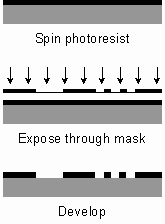
Micromachining requires some type of pattern transfer to turn designs into devices. By far, the most common type of pattern transfer in MEMS applications is the positive photolithography process, which is illustrated in Figure 2. In this process, a polymer called photoresist is deposited on the wafer and spun off; the spin speed controls the thickness of the layer. A reusable mask is placed over the wafer, and ultraviolet light is used to expose the photoresist. The mask is usually a glass or quartz plate with patterns printed in an opaque material such as chromium. Where the photoresist is exposed, a photochemical reaction causes it to become soluble in a developer, which is used to wash away the exposed areas. The remaining areas serve as a material mask for subsequent etch steps.
Figure 2. Photolithography process.
Surface micromachined devices are frequently fabricated from alternating polysilicon and silicon dioxide (oxide) thin films, as in the MUMPs(tm) [5] and SUMMiT(tm) [6] processes. These films, which are typically less than several microns thick, are deposited on the substrate through chemical vapor deposition. Between the deposition steps, the layers are patterned and etched to form the components of the desired device. The oxide layers are used to create spaces between the polysilicon structural layers, and the final step is the use of a hydrofluoric acid (HF) etch to dissolve the oxide and release the mechanical polysilicon devices.
The MUMPs and SUMMiT processes allow very complex devices to be fabricated. However, due to their inherent planar configuration, surface micromachined devices are not as robust as high-aspect-ratio devices. The thin structural layers are extremely compliant perpendicular to the wafer plane. Special environmental conditions are typically required to ensure consistent performance. Finally, residual stresses and stress gradients created in the films during deposition can often cause post-process deformation. Despite these disadvantages, multi-level processes are in widespread use due to their outstanding design flexibility.
A notable method of surface micromachining is thermal evaporation, often used to deposit thin metal films to provide conductive areas on a substrate. These areas provide bond pads and traces for electrical connectivity. Evaporators use a combination of resistive heating and very low pressures to boil or sublimate metals such as gold, chromium, and aluminum. Released molecules travel in a line-of-sight path to the intended target; pressures under 1 mTorr are required to prevent atmospheric scattering. Gold is often used as a conductive layer but will not adhere to the native oxide layer present on silicon; consequently, a thin intermediate layer of chromium or titanium is required [7].
Another type of micromachining is bulk micromachining, which encompasses both wet and dry etching. Both isotropic and anisotropic wet etching of silicon have been explored since the 1960s [4,8]. Microfabrication of SCS by anisotropic etching was particularly significant as it involves selective etching of certain crystalline planes. This capability allows the construction of 3-D devices such as nozzles and suspended beams [9]. However, device geometry is limited by the orientation of the crystalline planes. For example, cavities etched into <100>-oriented wafers feature inward sloping walls at an angle of 54.7 degrees. Trenches with vertical sidewalls can be etched into <110>-oriented wafers, but the shape and orientation of the trenches are constrained.
More recently, plasma-assisted dry etching has developed into a widespread bulk micromachining method. In particular, deep reactive ion etching (DRIE) can be used to etch high-aspect-ratio vertical trenches in silicon with depths exceeding several hundred microns. The mechanism of reactive ion etching is silicon removal by ion bombardment; the reactive gas used is SF6 [4]. DRIE is performed by alternating reactive ion etch steps with "passivation" steps [10]. During each passivation step, gaseous C4F8 is used to deposit a protective polymer film on trench sidewalls. The subsequent etch step removes the film preferentially from trench bottoms. As etching continues, the sidewalls are protected, allowing the creation of very deep trenches.
The advantage of DRIE is its ability to etch trenches of arbitrary shape and orientation with vertical sidewalls. However, there are some issues with the DRIE process. One problem, known as DRIE lag, is the fact that wider trenches are etched more quickly [11]. This problem is avoided if etching is continued down to a buried oxide layer. Oxide is selective against SF6 etching and is therefore suitable as an etch stop. However, two effects, known as bowing and footing, tend to reduce pattern dimensions through lateral overetching when etching SOI wafers [12]. These effects can be reduced by adjusting the duration of the etch and passivation steps.
Micromachining can be supplemented with other manufacturing steps such as wafer bonding. Silicon-on-insulator (SOI) wafers are in widespread use today [13,14]. These wafers consist of a silicon substrate several hundred microns thick and a thinner SCS layer known as the active layer. The active layer is frequently doped to a specified level of electrical conductivity. The two layers are separated by an insulating oxide layer commonly ranging in thickness from 0.1 to 4 microns.
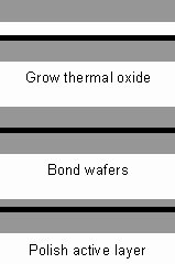
The most common process flow for manufacturing SOI wafers is shown in Figure 3. An oxide layer is grown on the first wafer from high-temperature exposure to a humid oxygen stream. Another wafer is then bonded to the first wafer and thinned by means of chemical-mechanical polishing. This polished wafer serves as the active layer. Considerable design flexibility can be achieved by varying the thickness of the oxide and active layers.
Figure 3. SOI wafer manufacturing.
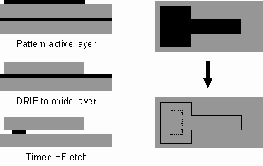
DRIE can be performed on an SOI wafer to produce suspended devices that are thermally and electrically insulated from the substrate. By incorporating HF etching, devices can be partially or completely undercut depending on etch duration. Figure 4 demonstrates the use of this technique to create a cantilever beam.
Figure 4. Creation of a cantilever beam by performing DRIE on an SOI wafer.
SOI wafers are manufactured by means of silicon fusion bonding, in which two wafers are bonded with no intermediate adhesive layer [15]. Bonding can occur spontaneously at room temperature from van der Waals attraction between two clean, polished wafers. However, the bonding surface energy at room temperature is less than 0.1 J/m2. In comparison, the fracture energy of bulk SCS is over 2.2 J/m2. High temperature annealing above 1000 °C is necessary to initiate viscous oxide flow and create strong Si—O—Si bonds that strengthen the wafer bond to the level of bulk SCS.
If both wafers are patterned, alignment is necessary before bonding. Mechanical alignment can be performed by using a jig [16] or fiber key [17]. More accurate alignment can be performed optically by using infrared light [18] or frontside and backside microscopes. Optical bond aligners that use light in the visible range require one wafer to be patterned with backside alignment marks. After loading the first wafer, a picture is taken of frontside alignment marks; this picture is stored while the second wafer is loaded over the first wafer. To align, backside marks on the second wafer are matched to the marks on the stored picture; the wafers are then contacted and annealed. Alignment errors of less than 10 mm can be achieved with optical aligners.
Wafer cleaning is a crucial part of bonding, as contaminants will create voids when the wafers are contacted. The most common cleaning method is the RCA treatment [19]. RCA1, a mixture of NH4OH, H2O2, and de-ionized (DI) water, dislodges foreign particles by simultaneously creating and dissolving an oxide film. RCA2, a mixture of HCl, H2O2, and DI water, is used to remove contaminants and to protect the silicon surface with an oxide film. If heavy organic contamination such as photoresist is present, the RCA treatment should be preceded by "piranha" cleaning with a combination of H2SO4 and H2O2. In all cases, cleaning is followed by rinsing with DI water. RCA1 also makes the silicon surface hydrophilic, which significantly promotes bonding [15]. For this reason, bonding is often preceded by an RCA1–RCA2–RCA1 treatment.