Back to table of contents | Next section
2.2 Overview of 3DMEMS Process
The 3DMEMS process uses two SOI wafers, DRIE, aligned wafer bonding, and HF etching to produce planar devices that are lifted out of the wafer plane prior to operation. The resulting spatial mechanisms are controlled in parallel by several single-DOF inputs. A planar process using only two wafers is employed to reduce the required number of alignment and bonding steps.
One of the notable features of the 3DMEMS process is the use of compliant beams as in-plane and out-of-plane joints. The macro-scale spatial manipulator shown in Figure 1 employs hinged, or revolute, joints. All revolute joints require some clearance between the hinge components. At the micro-scale, however, clearance dimensions can become comparable to device dimensions. For example, DRIE design rules typically require a minimum gap width of several microns. When many revolute joints are used, an accumulation of these clearances results in degraded positioning resolution. The 3DMEMS process replaces true revolute joints with flexural beams that are capable of deflection angles in excess of 45 degrees. These beams are used to form both in-plane and out-of-plane joints.
A part of the 3DMEMS research effort is concerned with modeling the behavior of compliant joints [2]. Because large deflections are encountered, linear beam theory is no longer applicable, and more complex models are required. One recently-developed model that has been applied to compliant MEMS devices is the pseudo-rigid-body model [31,32]. In the simplest version of this model, a compliant beam is replaced with two rigid links and one torsional spring, as shown in Figure 5. The primary objective of the model is to predict the torsional spring constant and the link lengths. Design can then continue as if rigid links were actually being used.
Figure 5. Compliant beam and equivalent pseudo-rigid-body model.
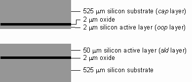
The two 3DMEMS SOI wafers are depicted in Figure 6. The top wafer is upside down so that the two polished active layers can be bonded. The names of the layers are indicative of their roles; for example, the sld layer is the primary structural layer, comprising the sliders and platform. The thin oop layer, which is bonded to the sld layer, provides out-of-plane joints. Finally, the cap layer holds the released structures in place.
Figure 6. SOI wafer configuration for 3DMEMS process.
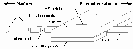
A conceptual 3DMEMS device that employs two out-of-plane joints and one in-plane joint is depicted in Figure 7. The oop layer is etched directly above the slider to provide clearance. The cap, guides, and slider comprise a prismatic joint.
Figure 7. Compliant and prismatic joints of conceptual 3DMEMS device.
The essential idea of the 3DMEMS process is that by means of the oop and cap layers, the top wafer provides both the compliant beams for out-of-plane joints and the caps that form prismatic joints with the sliders. The use of SOI wafers reduces the number of necessary alignment and bonding steps, simplifying the process and improving device yields. A timed HF etch is used to release the sliders while the anchors remain attached to the substrate.
A 3DMEMS device designed by Zhongzhou Tang of the 3DMEMS group is shown in Figure 8. This illustration is based on the actual 3DMEMS process flow, which will be discussed in the next section. In keeping with the batch fabrication requirements, the platforms of all the devices can be lifted off the substrate simultaneously after fabrication by using electrostatic attraction.
Figure 8. Compliant joints and platform of conceptual 3DMEMS device based on actual process flow.
Another feature of the 3DMEMS process is the bonding of patterned wafers. It has been shown that bonded patterned wafers can exhibit the same bond quality as bonded unpatterned wafers [14]. A study was performed as a part of the 3DMEMS research effort specifically to determine if bond quality depended on pattern size [33]. The width of the patterns varied from 10 mm to 185 mm. The surface energy of the bonds was consistently measured at about 2.1 J/m2, close to the fracture energy of bulk SCS. The study thus indicated that pattern size does not influence bond quality.