Back to table of contents | Next section
2.6 Revised 3DMEMS Process Flow
During the first fabrication run, some problems with the process were observed. Corresponding solutions were developed and incorporated to form a revised process flow. Fabrication problems and solutions are discussed in this section.
The first two problems with the process were relatively minor. First, the native oxide layer on the back of the 2 mm SOI wafer was thick enough to impede reactive ion etching in step 3 of Table 1. A process step was therefore added in which the wafer was dipped in HF to remove the oxide. The HF dip was performed until the backside was observed to be hydrophobic (oxide is hydrophilic, bare silicon is hydrophobic). Second, it was found that the 1 mm alignment marks etched in step 3 could not be identified because the unpolished substrate was too rough. Etch depths of 5 mm were attempted and found to be visible during subsequent alignment steps.
During the DRIE steps, wafers are transferred from a load chamber to an etch chamber by means of a robotic arm. During this transfer, wafers need to be perfectly centered on a load chuck. In the original process, however, the cap layer was not positioned at exactly the same wafer location as the sld layer; consequently, a slight wafer overlap was created during bonding that resulted in erratic wafer loading. To prevent overlaps from occurring, the lithography process was revised by switching steps 2 and 3 of Table 1 so the cap layer is patterned before the oop layer. Furthermore, the cap layer is patterned directly after and in the same wafer location as the sld layer. This solution was attempted on the second set of SOI wafers. The resulting wafer stack after bonding had no discernable overlap and could be loaded into the etch chamber reliably.
The 2 mm SOI wafer is patterned on both sides; however, the polished oop layer is easily damaged while the cap layer is being patterned. This damage is especially detrimental to the process because it occurs to a surface that will be bonded later. Initially, two photoresist layers were spun and baked onto the oop layer to protect it while the cap layer was being patterned. Unfortunately, the photoresist did not provide enough protection, and some damage was observed on the oop layer before bonding. On the second attempt, a 525 mm carrier wafer was temporarily bonded to the oop layer with photoresist before patterning the cap layer. The carrier wafer protected the oop layer sufficiently and was easily removed with acetone after RIE.
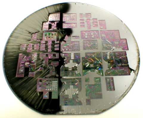
Bonding quality was a major issue in the first 3DMEMS fabrication run. Initial experiments involving patterned wafer bonding were successful [33]. Nevertheless, bonding during the first fabrication run was unsatisfactory. During DRIE of the cap layer, the wafers partially delaminated, as shown in Figure 14. The charring on the left side is believed to be caused by excessive heating after delamination occurred. During DRIE, the temperature of the wafer stack is regulated by a helium-cooled chuck. After delamination, however, the chuck could no longer effectively cool the top wafer. The other cap layer used in the first fabrication run broke in half during DRIE, probably due to similar thermal stresses.
Figure 14. Wafer stack showing thermal damage after final DRIE. Charring on the left side indicates overheating of the photoresist.
The original 3DMEMS process featured enclosed cavities around devices; it is believed that increased pressure in these cavities during annealing forced the bonded wafers apart. This effect was not discovered during the patterned bonding experiments because enclosed cavities were not studied. However, delamination has been observed by another group during annealing [34]. The following equation has been used to estimate the cavity diameter f that will cause delamination [adapted from 35]:
(1)
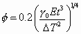
where g0 is the bonding energy at room temperature, E is the Young’s modulus of silicon, t is the thickness of the bonded wafer, and DT is the temperature change. Previous bonding experiments have estimated the bonding energy as 0.055 J/m2 [33]. By using a Young’s modulus of 166 GPa and an annealing temperature of 1000 °C, the critical diameter is calculated to be 6.8 mm. Some of the sealed cavities created during the 3DMEMS process are approximately 1 cm in diameter. Therefore, it is feasible that the wafers were forced apart during the annealing step.
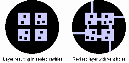
To solve the delamination problem, an extra mask has been produced (the vnt layer) that will be patterned over the sld layer. The vnt layer adds vent holes from all enclosed cavities to the edge of the wafer. These vent holes are expected to prevent delamination from excessive cavity pressure during annealing. It is hoped that thermal stresses will be reduced during DRIE, as the wafer stack will be sufficiently cooled. In Figure 15, a layer that results in sealed cavities is compared to a revised layer that adds vent holes.
Figure 15. Addition of vent holes to eliminate sealed cavities.
The revised 3DMEMS process steps are listed in Table 2.
Table 2. 3DMEMS revised process flow (P = pattern, AP = aligned pattern).
|
Step |
Layer |
Process |
Comments |
|
1 |
sld+vnt |
P / DRIE 50 mm |
Modified sld with vent holes |
|
2 |
cap |
HF etch |
Remove oxide layer |
|
3 |
oop |
Bond carrier wafer |
Bond with photoresist |
|
4 |
cap |
AP / RIE 5 mm |
Over sld; deeper marks |
|
5 |
oop |
Remove carrier wafer |
Remove with acetone |
|
6 |
oop |
AP / RIE 2 mm |
|
|
7 |
sld / oop |
Clean, bond |
|
|
8 |
cap |
AP / DRIE 525 mm |
|
|
9 |
all |
HF etch |
|